Highlight/Core Technology
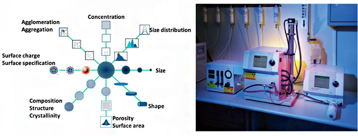
Measurement and calibrations of the micro- and nano-particles: sizes, size distribution, morphology, number concentration, and other important parameters, using calibrations systems based on optical, electric-gravity balance, electron microscope and other methods.
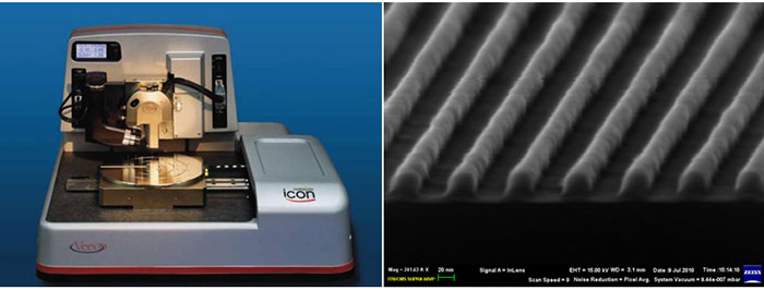
Nanoscale measurement and calibrations for critical dimensions of semiconductor industry: the critical dimensions include gratings, pitches, and line widths using atomic force microscope and electron microscope.
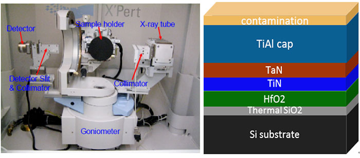
Thin film thickness measurements: calibrations of micro- and nano-scale film thickness using spectroscopic ellipsometry and grazing incidence X-ray reflectometry
Introduction
The standards established by the Laboratory include nanoscale Critical Dimension standards, micro-and nano-particle standards and semiconductor metrology standards to meet domestic measurement and traceability needs in the fields of nanoscale, semiconductor industry and so on.
- Provide nanoscale Critical Dimension standards to semiconductor industry for advanced manufacturing process requirements such as pitches, line widths and ultra-thin film thickness to assure the measurement quality, and improve the production of yield rate.
- To meet the measurement requirements of the particle size and number concentrations in the semiconductor manufacturing processes for improving the quality and yield of advanced fabrications.
Research Projects
- Establishment of calibration systems for semiconductor critical dimensions
In advance process control for semiconductor manufacturing beyond 7 nm technology node, the measurement requirements for pitch (line spacing) and the line width have come to 21 nm and 14 nm respectively. Currently, it is urgent for NML to provide the measurement traceability and calibrations, since there are no such reference standards for the pitches and the line widths. At the same time, the semiconductor industry have required overlay measurements with less than 0.5 nm in the resolution, and the film thickness measurements with less than 1 nm. However, the current optical scattering methods are encountered their measurement limits. Therefore, the project is aimed to provide calibrations and reference standards for the CDs, film thickness and overlay measurements. Based on X-ray technology, combined with atomic force microscopy measurement technology, the development of grazing incidence X-ray fluorescence spectroscopy (GIXRF) provide and expand the film thickness measurement down to 1 nm, and improve the accuracy of measurement. In addition, the development of grazing incidence small angle X-ray scattering (GISAXS) technology, expand the pitches and line widths measurements down to 21 nm and 14 nm below, respectively. For calibration purpose, it is also important to develop reference standards for both pitches and line widths in order to disseminate the standards to semiconductor industry. The development of GISAXS technology can also provide Overlay issue in semiconductor industry with resolution down to 0.5 nm.
- Critical dimensions calibration systems and measurements in both micro- and nano-scales
- Film thickness, pitch standards and linewidth standards (Atomic force Microscopy, X-Ray Reflectometry, Spectroscopic Ellipsometry)
- Dissemination and calibration of Film thickness, pitch standards and linewidth standards for establishing measurement traceability
- Establishment of calibration systems for nanoparticles
Semiconductor manufacturing processes are very sensitive to very small amounts of contaminations in all process generated by the solvents or gases, such as oxygen, water gas, carbon dioxide, particulates, transition metals or heavy metals. Semiconductor manufacturers are required to pay attention to particle contaminations that may be encountered by chemicals used in each process step. In the advanced manufacturing processes, the particle size of the killer particles that caused the defect is down to 9 nm, according to a report by the 2017 International Roadmap for Devices and Systems (irds). It is expected to be down to 6 nm in 2021 continuously. In response to the need to detect the particle size of 6 nm in the manufacturing processes, the project is to establish "technology of nano-particle analysis and standards." The measurement technology intends to cover the developments of particle size < 20 nm, particle concentration < 106 cm-3 and composition analysis.
- Calibration and measurement systems for nanoparticle related measurement parameters, such as
Nanoparticle sizes
Specific areas
Zeta potentials
Number concentrations
Compositions (organic and inorganic)
Impurity
- Dissemination and calibration of nanoparticles related standards for establishing measurement traceability
Technical Services
- Film thickness standards (1.5 nm to 1000 nm)
- Pitch standards (50 nm to 25 µm)
- Linewidth standards (50 nm to 1000 nm)
- Nanoparticle specific surface area (550 m2/g to 4000 m2/g)
- Polystyrene nanoparticle Zeta potential (nanoparticle size 10 nm to 20 nm: -75 mV < Zeta potential < 75 mV ,)
- Polystyrene nanoparticle size standards (10 nm to 1000 nm)
- Nanoparticle size standards (1 nm to 1000 nm)
- Nanoparticle number concentrations: number concentrations (size 100 nm: 1 particle/L, Class 1 clean room)
- Nanoparticle number concentrations: number concentrations (< 104 particles/mL) (size 100 nm: 1 cm-3 to 1000 cm-3;size 50 nm to 200 nm: 1000 cm-3 to 10000 cm-3)
- Nanoparticle impurity analysis: nanoparticles, number concentrations, and organic/inorganic compositions in semiconductor specialty gases, ultra-pure water and electronic grade chemicals.